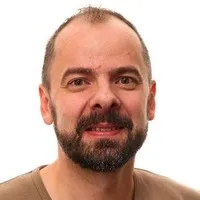
Timeline
About me
Electronic Development Engineer
Education

Technical university of denmark (dtu)
2000 - 2004Bachelor of science (bsc) electrical and electronics engineering (ee) grade point average: 9.4
Experience
Capres a/s
Jan 2005 - Mar 2017Electronic development engineerResponsibilities with the semi and full-automated tools from a to z: Development: Design of hardware and firmware, economic evaluation, optimization, simulating, layout and testing of electronics. In addition, develop, test, and optimize the performance of the completed semi and full-automated tools.Documentation: Schematic/layout of the electronic, and Schematic of the electronic modules, BOM list (Bill of materials), production and test instructions. Production: In house production. Outsourcing to Danish sub-supplier, EMS (Electronics manufacturing services), to make electronic modules for the tools. In addition, outsourcing to USA sub-supplier to build the semi and full-automated tools. Continuing service to sub-suppliers to optimize production. Cooperation with different departments: software, mechanical, service, physics, application and sale, to optimize the customer’s tools usage.Results:MicroRSP-A300: Full-automatic, micro scale resistivity measurements of 300 mm wafers, for semiconductor industry.CIPTech-M300: Half-automatic, micro scale, measures Magneto-resistance and Tunnelling Resistance (MR and RA) directly on blanket Magnetic Tunnel Junction (MTJ) for semiconductor industry and universities.MicroHALL-A300: Full-automatic, micro scale, Hall mobility, active carrier density, measurements of 300 mm wafers for semiconductor industry.MicroHALL-M300: Half-automatic version for semiconductor industry and universities.M4PP SEM Module: micro- and nanoscale conductivity measurements on a wide range of materials and devices in a Scanning Electron Microscope (SEM) or Focused Ion Beam (FIB).Thick and thin metal film module to full-automatic A300 tool: From micrometres to angstroms metal film layer. E.g. 5 angstroms gives a few atoms thin metal film layer, doped on a wafer.Scientific papers, co-author, in cooperation with DTU. Show less
Danisense a/s
Apr 2017 - nowR&d engineerDevelopment with high accuracy current transducers.
Licenses & Certifications
- View certificate

Prince2
Apm groupJul 2010
Languages
- daDanish
- enEnglish
Recommendations

Lisette raud
Marketing Project Manager at Rahva Raamat ASTallinn, Harjumaa, Estonia
Kent li
General Manager at Atlas Copco - Factory for Industrial Air Compressors (Jiangmen) Co., Ltd.Baoshan District, Shanghai, China
Haley guildford
Creative at Haley Guildford PhotographerAuckland, Auckland, New Zealand
Tareq hasan
Information Technology Project Manager at LänsförsäkringarStockholm, Stockholm County, Sweden
Ľubka petrášová gbelcová
Product manager/Product Owner/BABratislava, Bratislava, Slovakia
Daniel watanabe
eLearning Researcher, Innovator, Designer, EntrepreneurSeongdong District, Seoul, South Korea
Ross lumsden
ROV Pilot / Tech 2 Director EML Engineering LtdElgin, Scotland, United Kingdom
Shubham bawaskar
HRBP at Cipla | Ex RILPune, Maharashtra, India
Jeffrey hill
Global Tax Partner - EYIselin, New Jersey, United States
Oliver coley
Senior Software DeveloperReston, Virginia, United States
...
 Deep Enrich